Introduction
The Fujifilm Dholera semiconductor materials story has developed significantly during 2026.
On 30 June 2026, FUJIFILM India announced an MoU with the Gujarat State Electronics Mission to explore semiconductor-materials manufacturing opportunities in India and assess the possibility of establishing a production base in Dholera.
On 2 September, the company reinforced that direction ahead of SEMICON India 2026, highlighting its semiconductor-materials expertise, localisation plans and CMP slurry technology.
Then came the most important development.
On 17 September 2026, Fujifilm and Tata Electronics announced a strategic MoU focused specifically on building the semiconductor-materials ecosystem around Tata Electronics’ upcoming Dholera semiconductor fab. Fujifilm also announced that it plans to invest approximately ₹800 crore to establish a semiconductor-materials plant in
Dholera Special Investment Region in phases.
That changes how the story should now be described.
Fujifilm is no longer only evaluating whether semiconductor-materials manufacturing could be established in Dholera. There is now an announced investment plan and a strategic relationship with Tata Electronics.
However, an announced plant is not the same as a plant already under construction or in operation.
As of 24 September 2026, the official releases reviewed for this article do not provide a confirmed construction-start date, commissioning date, production capacity, employment number or commercial-production date for Fujifilm’s proposed Dholera plant.
This article explains exactly what has been announced, what semiconductor materials actually are, how the proposed Fujifilm facility fits alongside Tata’s chip fab and which future milestones would show that the project has moved from announcement to physical implementation.
What Has Fujifilm Announced About Dholera?
The Fujifilm Dholera story can be understood through three important announcements.
30 June 2026 — Gujarat MoU and Dholera Evaluation
FUJIFILM India announced that it had signed a Memorandum of Understanding with the Gujarat State Electronics Mission (GSEM), Department of Science and Technology, Government of Gujarat.
The stated objective was to explore opportunities for semiconductor-materials manufacturing in India and strengthen domestic semiconductor supply chains.
Importantly for Dholera, Fujifilm said it intended to assess opportunities to establish a semiconductor-materials production base in Dholera.
The wording mattered.
At that stage, the announcement established serious interest and formal cooperation, but it did not establish that a manufacturing plant was already under construction or operating.
2 September 2026 — Semiconductor Materials Focus Reinforced
Fujifilm’s next major India announcement came ahead of SEMICON India 2026.
The company said it would showcase its semiconductor-materials portfolio and global technology capabilities at the event while highlighting localisation, customer partnerships and semiconductor supply-chain development in India.
Fujifilm specifically highlighted its CMP slurry technology, which is used in precision semiconductor manufacturing.
The September announcement also referred back to the June Gujarat MoU and confirmed that the company continued to explore opportunities to bring its technologies and manufacturing expertise closer to the Indian market.
The 2 September release therefore strengthened the semiconductor-materials story, but still did not by itself establish an operational Dholera plant.
17 September 2026 — Tata Partnership and ₹800 Crore Dholera Plant Plan
The most significant development came during SEMICON India 2026.
Tata Electronics and Fujifilm announced a strategic MoU designed to accelerate development of the semiconductor-materials ecosystem in India, particularly around
Tata Electronics’ Dholera fab.
According to the companies, Fujifilm plans to develop and supply advanced semiconductor materials tailored to the requirements of Tata Electronics’ upcoming semiconductor fab.
The companies also said they intend to strengthen supply-chain resilience by localising critical raw materials and supporting Indian chemical manufacturers with technology, quality assurance and manufacturing-process know-how.
Most importantly, Fujifilm announced that it will strategically invest approximately ₹800 crore to establish a semiconductor-materials plant in Dholera Special Investment Region in phases.
That is much more specific than the June evaluation-stage announcement.
Fujifilm Dholera Project: What Is Confirmed Today?
As of 24 September 2026, the clearest status can be summarised like this:
The most accurate description today is therefore:
Fujifilm has announced an approximately ₹800 crore phased semiconductor-materials plant for Dholera SIR and a strategic materials partnership with Tata Electronics, but the plant should not yet be described as operational unless a later official announcement confirms commissioning or commercial production.
What Is a Semiconductor Materials Facility?
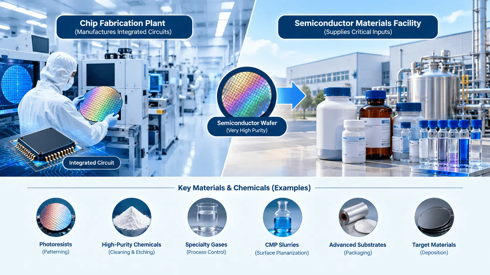
A semiconductor-materials facility is very different from a semiconductor chip fabrication plant.
A chip fab manufactures integrated circuits on semiconductor wafers through many extremely controlled processing stages.
Those manufacturing stages require specialised materials and chemicals with extremely high levels of purity and consistency.
A semiconductor-materials company supplies some of those critical inputs.
FUJIFILM Electronic Materials globally produces materials used across semiconductor manufacturing and packaging. Its wider portfolio includes products such as:
This does not mean that every product in Fujifilm’s global portfolio has been confirmed for manufacture at Dholera.
The exact product mix and manufacturing capacity of the proposed Dholera facility have not yet been publicly detailed in the official releases reviewed for this article.
That distinction is important.
What Is CMP Slurry and Why Did Fujifilm Highlight It?
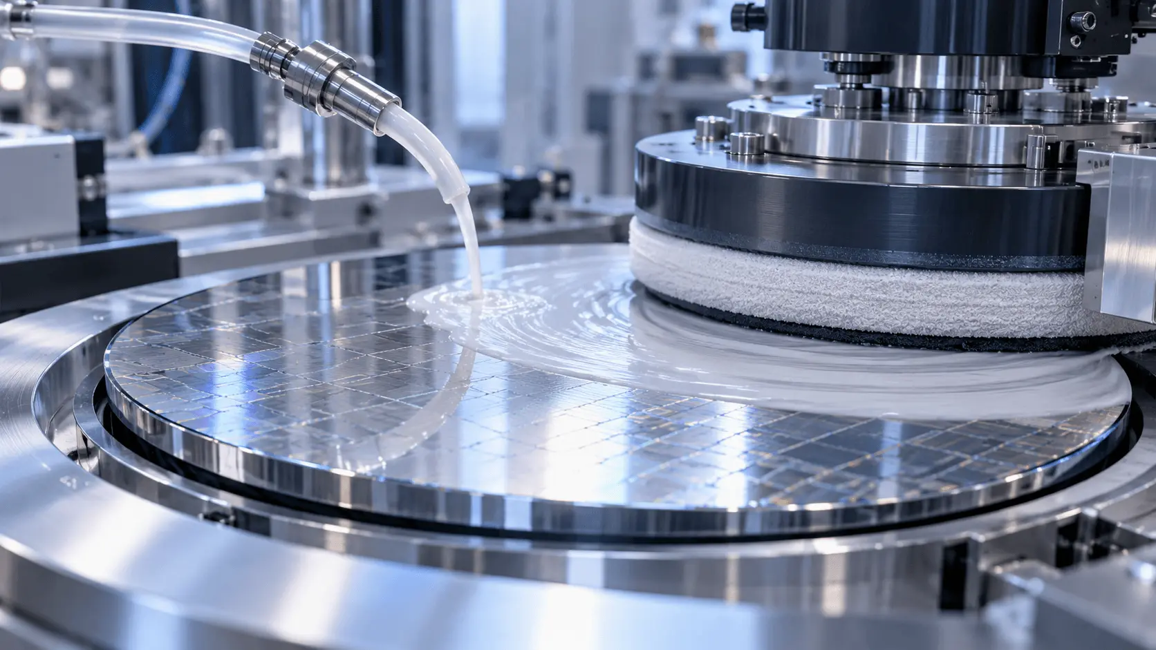
CMP stands for Chemical Mechanical Planarization.
During semiconductor manufacturing, many extremely thin material layers are deposited and patterned on a wafer.
The wafer surface needs to remain exceptionally flat as these layers are built.
CMP combines chemical action with mechanical polishing to remove selected material and create a highly controlled flat surface for later manufacturing stages.
The specialised chemical mixture used in this process is known as a CMP slurry.
Fujifilm supplies different CMP slurry solutions for semiconductor applications, including materials related to copper, barrier metals, front-end processing and advanced packaging.
Fujifilm’s 2 September SEMICON India announcement specifically highlighted CMP slurry technology as an example of its semiconductor-materials capabilities.
Again, that technology showcase should not automatically be interpreted as confirmation that every Fujifilm CMP product will be manufactured in Dholera.
The local product portfolio will need to be confirmed through subsequent company announcements.
How Does Fujifilm Fit Alongside Tata's Dholera Semiconductor Fab?
This is one of the most important distinctions in the Dholera semiconductor ecosystem.
Tata Electronics is building the semiconductor fabrication facility.
Fujifilm’s proposed business role is to supply and potentially manufacture specialised materials required by semiconductor manufacturing.
Tata’s Dholera project is being developed as a 300 mm semiconductor fab, with technologies planned across approximately 28 nm to 110 nm and total investment stated at around ₹91,000 crore.
Fujifilm sits at a different layer of the manufacturing chain.
A simplified relationship looks like this:
Semiconductor raw materials and specialised chemicals → wafer-fabrication processes → semiconductor wafers/chips → packaging, testing and downstream electronics
Fujifilm is positioned toward the materials side of this chain.
Tata is positioned at the wafer-fabrication side.
The 17 September agreement links those two layers directly.
Fujifilm said its advanced materials would be developed and supplied according to the requirements of
Tata Electronics’ Dholera fab, while localisation is intended to strengthen the availability and movement of semiconductor materials.
Why Is Local Semiconductor-Materials Manufacturing Important?
Building a semiconductor fab is only one part of creating a semiconductor manufacturing ecosystem.
A fab also depends on reliable access to:
high-purity chemicals, specialty materials, gases, advanced manufacturing equipment, cleanroom systems, process-control technologies, engineering services, maintenance capabilities, logistics and trained manpower.
Some semiconductor materials must meet extraordinarily strict contamination and quality requirements.
For that reason, supply reliability, quality control and consistent material specifications are critical.
The stated Fujifilm–Tata collaboration focuses on localisation and supply-chain resilience rather than simply importing every critical material from overseas.
Fujifilm also said the partnership would support Indian chemical manufacturers through technology, quality assurance and manufacturing-process expertise.
This is an important development because it suggests that the Dholera semiconductor story is expanding from a single fab toward supporting industries around that fab.

Fujifilm Is Different From Tata, PSMC, ASML and Crystal Matrix
Several semiconductor-related company names are now associated with Dholera, but they should not be treated as interchangeable.
Understanding these different roles gives a much clearer picture of what an actual semiconductor ecosystem looks like.
It is not simply several companies building the same type of factory.
They can occupy different positions across materials, equipment, wafer fabrication, advanced displays, packaging, technology and supporting services.
Does the ₹800 Crore Announcement Mean Construction Has Started?
No such conclusion should be made from the investment announcement alone.
The 17 September release confirms that Fujifilm plans to invest approximately ₹800 crore and establish its semiconductor-materials plant in Dholera SIR in phases.
However, an investment announcement or MoU is different from physical construction commencement.
The reviewed official releases do not specify a construction-start date.
Until a later dated source confirms physical implementation, it is better to describe the project as an announced/planned semiconductor-materials plant rather than a completed or operating factory.

Which Future Announcement Would Confirm That Construction Has Started?
Several types of future evidence could materially change the project’s status.
A strong construction milestone could include an official Fujifilm or Tata Electronics announcement of groundbreaking or construction commencement, a formally identified project site together with commencement activity, a major construction/EPC award associated with the facility, or another authoritative government/company disclosure establishing that physical plant development has started.
The important principle is that the source should identify a real implementation milestone rather than simply repeat the ₹800 crore investment announcement.
Until then, “planned” or “to be established” remains safer language.
What Would Confirm That the Fujifilm Dholera Plant Is Operational?
An operational milestone would require a stronger form of evidence.
Examples could include an official announcement of:
plant commissioning, start of production, commencement of commercial manufacturing, completion of a manufacturing phase, first qualified production, or first commercial supply from the Dholera facility.
A later company announcement confirming that locally manufactured material from the Dholera plant is being supplied to customers or to Tata Electronics would also be significant evidence of operational progress.
Without such confirmation, phrases such as “Fujifilm’s operational Dholera plant” or “production has started” should be avoided.
Why Does the Fujifilm Announcement Matter for Dholera?
The importance of Fujifilm is not only the ₹800 crore investment figure.
The more important development is the type of industrial activity being proposed.
Dholera already has a major semiconductor fab being developed by Tata Electronics.
A materials manufacturer planning to locate nearby suggests a second layer of the semiconductor value chain may develop around that anchor facility.
If additional suppliers in materials, gases, equipment, logistics, maintenance, packaging and other specialist services establish operations around the fab over time, Dholera could develop a broader manufacturing cluster rather than remain dependent on one semiconductor project.
But that development should be measured through actual investments, facilities, hiring and production rather than assumptions.
Does the Fujifilm Plant Guarantee Higher Property Prices in Dholera?
No.
Industrial investment can be relevant when analysing the long-term economic development of a region, but the announcement of a factory does not guarantee property appreciation.
A particular land parcel still needs to be evaluated according to factors such as:
location, legal title, applicable zoning, TP Scheme or Final Plot details, permitted land use, existing and planned road access, surrounding development, approvals, pricing and investment horizon.
The Fujifilm announcement can therefore be treated as evidence of the development of Dholera’s industrial ecosystem.
It should not be treated as evidence that every nearby private plot will appreciate or that every project marketed using the words “
semiconductor” or “Fujifilm” is connected with the company.
Frequently Asked Questions
Conclusion
The Fujifilm Dholera semiconductor materials story has moved rapidly during 2026.
What began in June as an MoU to assess semiconductor-materials manufacturing opportunities in Gujarat and evaluate Dholera as a production base became considerably more specific in September.
The 17 September 2026 Fujifilm–Tata Electronics announcement now establishes a strategic materials partnership around Tata’s Dholera fab and an announced Fujifilm investment of approximately ₹800 crore for a phased
semiconductor-materials plant in Dholera SIR.
That is an important development for Dholera because semiconductor manufacturing requires much more than a wafer fab. It requires a surrounding network of materials suppliers, equipment companies, chemical manufacturers, engineering businesses and other specialised partners.
Fujifilm potentially represents one of those supporting layers.
At the same time, accuracy matters.
The ₹800 crore announcement confirms an investment plan. It does not by itself prove that construction has started or that a manufacturing plant is already operational.
The next phase of the story should therefore be judged through dated evidence of site development, construction, capacity, commissioning and eventual production.
For people following Dholera, that distinction gives a much clearer picture of how the semiconductor ecosystem is actually developing.
Official Sources Reviewed
This article was prepared using Fujifilm’s 30 June 2026 announcement regarding its MoU with the
Gujarat State Electronics Mission; Fujifilm’s 2 September 2026 SEMICON India announcement; and the 17 September 2026 Fujifilm–Tata Electronics strategic partnership announcements issued by Fujifilm and Tata Electronics. Fujifilm’s official semiconductor-materials information was also reviewed to explain the role of products such as CMP slurries and other process materials.
Disclaimer
This article is intended for educational and informational purposes only and reflects publicly available information reviewed up to 24 September 2026.
Fujifilm’s announced investment, manufacturing plans, product portfolio, project phases, construction schedule, production capacity and commissioning timeline may change as the project progresses.
References to FUJIFILM Corporation, FUJIFILM India, Tata Electronics, Gujarat State Electronics Mission, Government of Gujarat or any other organisation do not imply a partnership, endorsement or commercial association with Dholera City Buildconz.
Dholera City Buildconz is an independent real estate business and is not affiliated with Fujifilm, Tata Electronics, DICDL, DSIRDA or any government authority.
Industrial announcements should not be interpreted as a guarantee of real-estate appreciation, rental demand, resale liquidity or investment returns. Buyers should independently verify property title, zoning, approvals, access, applicable planning records and current government information before making a property decision.