Introduction
Dholera’s semiconductor story is no longer only about Tata Electronics.
In May 2026, the Government of India approved another semiconductor manufacturing project for
Dholera—this time from Crystal Matrix Limited (CML).
But the Crystal Matrix Dholera project is technically very different from Tata’s large silicon
semiconductor fab.
Crystal Matrix plans an integrated compound semiconductor fabrication and ATMP facility focused
on Gallium Nitride, or GaN, technology and Mini/Micro-LED display modules. The Union Cabinet
approved the project under the India Semiconductor Mission on 5 May 2026.
Instead of treating this as another generic “semiconductor investment in Dholera” story, it is more
useful to understand what the plant is actually designed to make.
What Is the Crystal Matrix Project in Dholera?
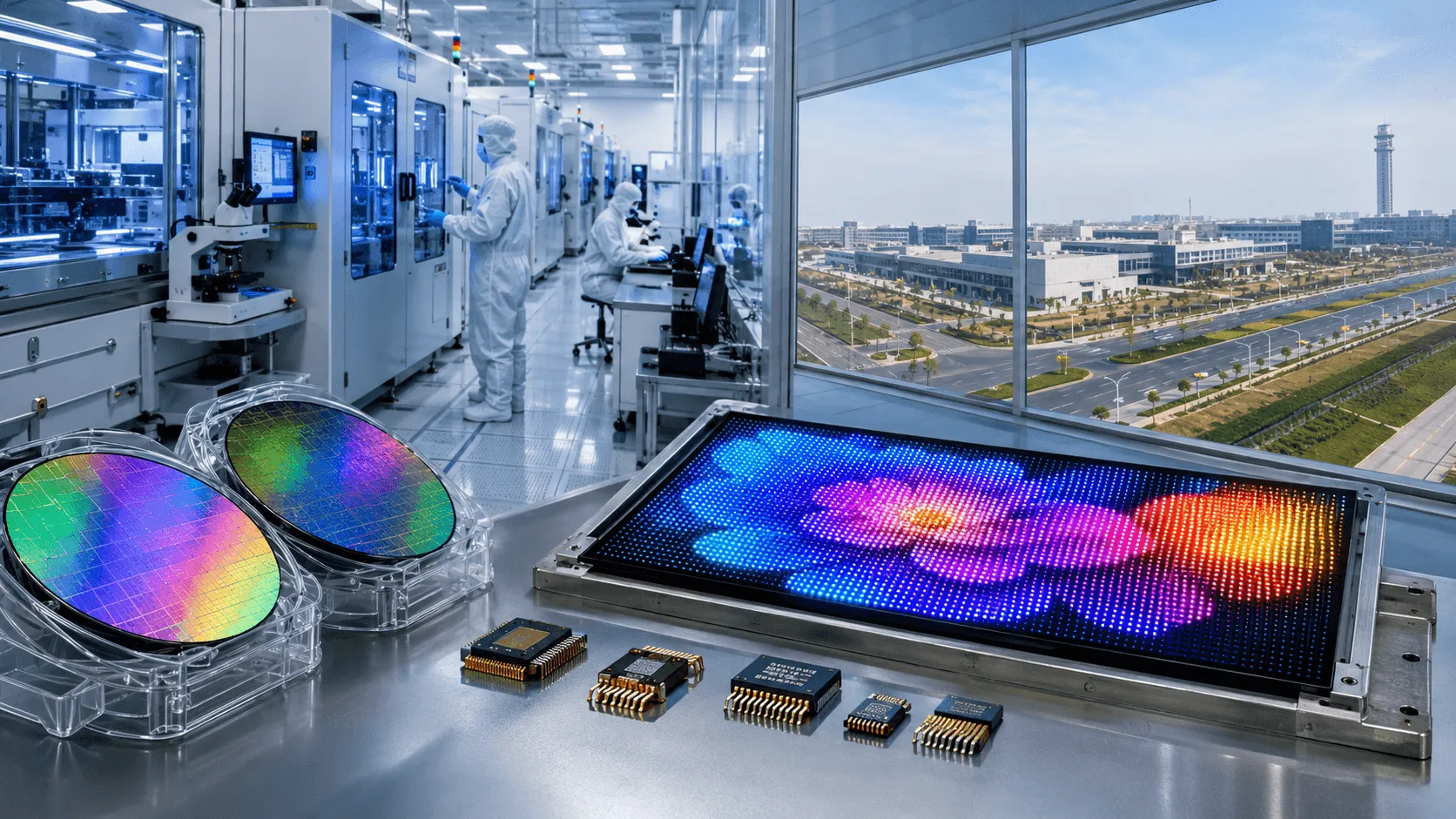
Crystal Matrix Dholera is an approved compound semiconductor and advanced display
manufacturing project that plans to produce GaN epitaxy wafers and Mini/Micro-LED display
products in Dholera, Gujarat.
According to the Government of India, Crystal Matrix Limited will establish an integrated compound
semiconductor fabrication and ATMP—Assembly, Testing, Marking and Packaging—facility at
Dholera.
The government-approved project has an estimated cost of approximately ₹3,068 crore. Official project
information lists proposed annual capacity of 72,000 square metres of Mini/Micro-LED display panels
and 24,000 sets of RGB GaN epitaxy wafers, along with direct employment for about 1,600 people.
This makes Crystal Matrix important not simply because it is another factory in Dholera, but because it
introduces a different branch of semiconductor manufacturing: compound semiconductors and
optoelectronics for advanced displays.
The production figures and investment above are proposed project capacities disclosed by the
Government of India; they should not be interpreted as current production output.
What Will the Crystal Matrix Dholera PlantActually Make?
Understanding the project becomes easier if we look at it as a manufacturing chain rather than simply
calling it a “semiconductor plant.”
A simplified process looks like this:
GaN material → epitaxy wafer → tiny LED devices → packaging and assembly → Mini/Micro-LED
modules → finished display panels
Crystal Matrix says its Dholera facility is being established to manufacture and process 6-inch GaN
epitaxy wafers and integrate downstream Mini/Micro-LED display manufacturing. The company also
describes an ATMP facility for advanced display modules and panels.
Each part of that chain deserves some explanation.
What Is GaN Semiconductor Technology?
GaN stands for Gallium Nitride. It is a compound semiconductor material with properties that
make it useful in high-performance electronics and optoelectronic devices such as LEDs.
Most people associate semiconductor manufacturing with silicon. Silicon remains the dominant
material for processors, controllers and many other integrated circuits.
GaN belongs to a different family.
It is made from gallium and nitrogen and is classified as a wide-bandgap semiconductor. GaN has a
bandgap of about 3.4 eV, compared with roughly 1.1 eV for silicon. Wide-bandgap materials can
support applications requiring high efficiency, high frequency, higher temperature operation and,
importantly for this project, efficient light emission.
GaN is already a fundamental material behind modern high-efficiency LEDs. Its optical properties are
one reason it is highly relevant to next-generation Mini-LED and Micro-LED technology.
So when people hear GaN semiconductor Dholera, they should not automatically imagine the same
type of chips made in a conventional silicon logic fab.
In the Crystal Matrix project, GaN is closely connected with the production of tiny light-emitting
semiconductor devices for advanced displays.
What Does “GaN Epitaxy Wafer” Mean?
This is one of the technical terms buyers and general readers may see in reports about Crystal Matrix.
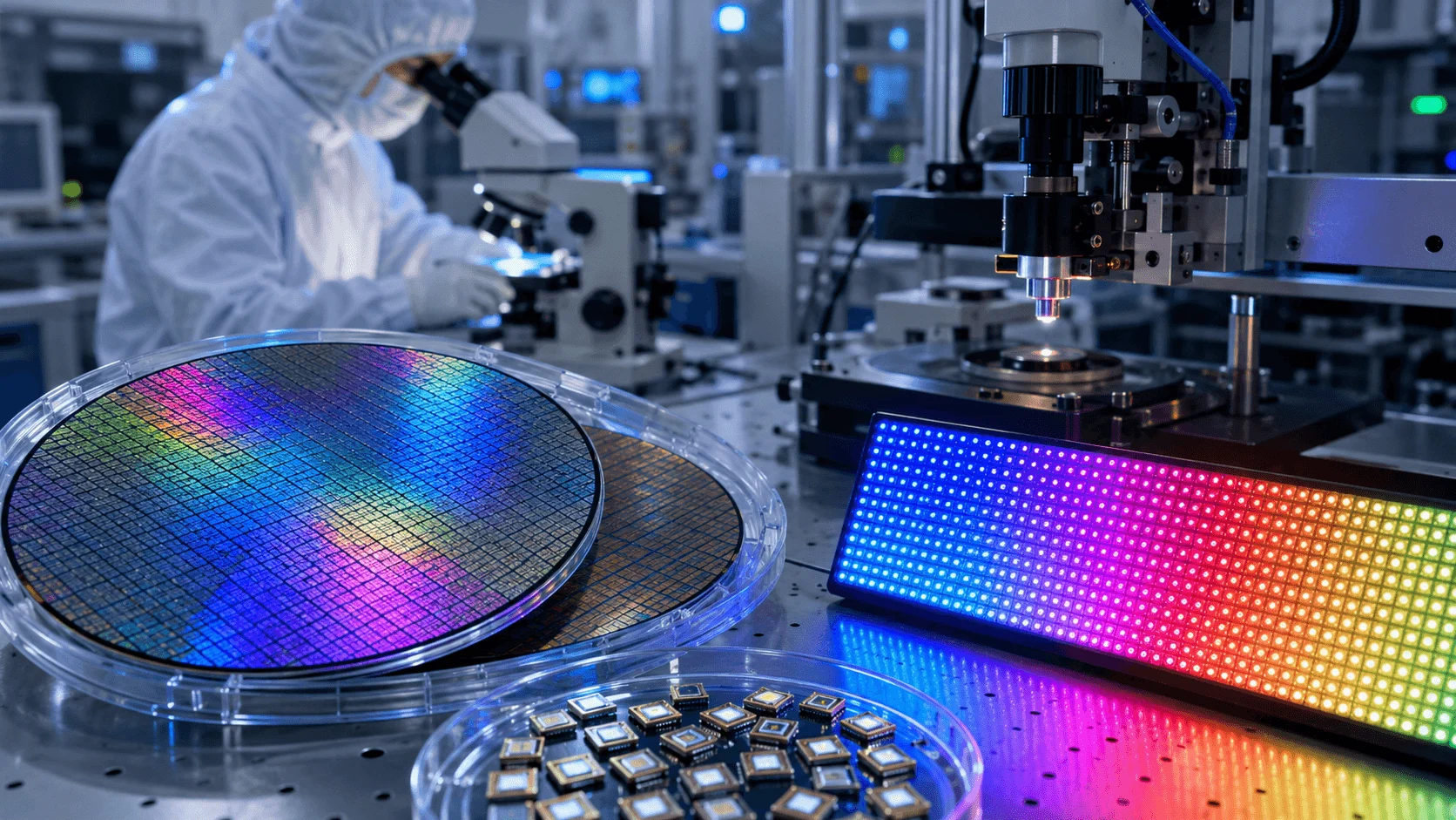
Epitaxy is the process of growing carefully controlled crystalline semiconductor layers on top of a
wafer or substrate.
Those layers are engineered to give the semiconductor device the electrical and optical characteristics it
needs.
You can think of a wafer as the foundation, while epitaxy creates the precisely engineered
semiconductor layers from which functional LED devices can later be fabricated.
The Government’s Crystal Matrix announcement specifically says the integrated facility will provide GaN
foundry services including epitaxy on 6-inch wafers.
That is significant because it means the project is intended to go deeper into the semiconductor
manufacturing chain than simply importing finished LED chips and assembling them into screens.
What Are Mini-LEDs?
Mini-LED refers to very small LED devices used to provide finer and more precise control of light in
display systems.
In consumer televisions and monitors, the term Mini-LED commonly describes an advanced LCD
backlight containing many much smaller LEDs than a conventional LED-backlit LCD.
Because more LEDs can be placed behind the panel, manufacturers can create many local-dimming
zones. That allows brighter highlights, improved contrast and better control over dark areas of an
image compared with simpler LCD backlights.
However, there is an important technical nuance when discussing the Dholera Mini LED plant.
Mini-LED is not limited to consumer-TV backlighting terminology. Tiny LED chips can also be integrated
into advanced direct-view display modules using packaging approaches such as Chip-on-Board (CoB).
Crystal Matrix specifically describes its planned Dholera ecosystem as producing Mini/Micro-LED
modules and panels using advanced packaging approaches, so it is better to understand the project as
an advanced LED display manufacturing platform, rather than simply as a television-backlight
factory.
What Is Micro-LED?
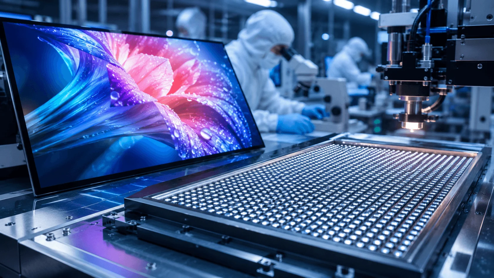
Micro-LED is a self-emissive display technology in which microscopic semiconductor LEDs
generate the light used to form the image.
This is fundamentally different from a conventional LCD.
An LCD requires a light source behind the liquid-crystal layer.
In a Micro-LED display, tiny LEDs themselves can function as the individual light-emitting elements.
Because the light is generated directly at the pixel level, Micro-LED technology has the potential to
combine very high brightness, strong contrast, fast response and long operating life.
This sounds simple in theory.
Manufacturing it at scale is not.
A high-resolution screen may require an enormous number of microscopic LED elements to be
fabricated, tested, transferred, connected and packaged with extremely low defect rates.
That manufacturing difficulty is one of the reasons Micro-LED remains an advanced—and challenging—
display technology.
Micro-LED pushes LED dimensions, integration density and manufacturing precision considerably
further.
What Is ATMP in the Crystal Matrix Project?
ATMP stands for:
Assembly, Testing, Marking and Packaging.
A semiconductor device does not become a usable finished product immediately after fabrication.
It usually has to be separated or integrated, electrically connected, packaged, tested and prepared for
use in a larger electronic system.
For Crystal Matrix, this downstream capability is especially relevant because the project is not only
about producing semiconductor material.
It also plans to integrate those semiconductor devices into Mini/Micro-LED display modules and
panels. The company describes CoB and CoG display-panel capabilities as part of its planned
manufacturing ecosystem.
In other words, the project attempts to connect semiconductor fabrication with advanced display
manufacturing within one broader ecosystem.
What Could the Dholera Micro LED Project BeUsed For?
The Government of India says the proposed Crystal Matrix products can serve several display
categories.
They include large displays for televisions and commercial signage, medium-sized screens for
smartphones, tablets and automotive applications, and smaller displays for devices such as XR glasses
and smartwatches.
A separate official project summary also mentions applications such as large video walls, AR/VR, studio
production, ruggedised displays and medical uses.
This range is important.
The Crystal Matrix semiconductor Gujarat project is therefore not centred on one consumer product.
Its underlying technology can potentially feed multiple display markets—from very large professional
screens to extremely compact wearable displays.
Is the Crystal Matrix Dholera Project Approved?
Yes. The Crystal Matrix Dholera project received Union Cabinet approval under the India
Semiconductor Mission on 5 May 2026.
The official announcement described Crystal Matrix as one of two additional semiconductor
manufacturing proposals approved in Gujarat and identified the Dholera project as India’s first
commercial Mini/Micro-LED display facility based on GaN technology.
However, approved does not mean operational.
As of 31 August 2026, the publicly available Crystal Matrix information describes the facility as being
established. Therefore, it is more accurate to describe Crystal Matrix as an approved or planned/
being-established manufacturing project, unless a later official announcement confirms
commissioning or commercial production.
That distinction is important for accurate reporting.
Is Crystal Matrix the Same Type ofSemiconductor Fab as Tata?
No. Crystal Matrix and Tata Electronics are building very different semiconductor manufacturing
facilities in Dholera.
Both belong to the semiconductor ecosystem, but they focus on different materials, manufacturing
platforms and end products.
Crystal Matrix Dholera vs Tata Semiconductor Fab
Tata Electronics says its Dholera facility is being built as a 300 mm semiconductor foundry with
planned capacity of 50,000 wafers per month and process technologies ranging from 28 nm to 110 nm
for analog and logic chips.
Crystal Matrix, in contrast, is focused on GaN-based compound semiconductors and the Mini/Micro-LED
display ecosystem.
One important caution: the capacity figures in the table are not directly comparable. Tata’s capacity is
measured in silicon wafer starts per month, while Crystal Matrix’s published capacity uses display area
and sets of RGB epitaxy wafers.
They are different manufacturing businesses.
Why Can Dholera Host Both Types ofSemiconductor Projects?
Other companies may handle packaging, specialty gases, materials, equipment, components or
downstream electronics.
From that perspective, Tata and Crystal Matrix are more useful to understand as complementary
pieces of a manufacturing ecosystem, rather than as two competing versions of the same fab.
Crystal Matrix adds an advanced display and GaN optoelectronics dimension to Dholera’s
semiconductor profile.
Why Crystal Matrix Matters Beyond the ₹3,068Crore Investment Number
Large investment numbers often dominate headlines, but they do not explain why a technology project
matters.
The more interesting part of Crystal Matrix is the proposed combination of:
GaN epitaxy + compound semiconductor fabrication + advanced packaging + Mini/Micro-LED
display manufacturing.
If executed as proposed, this represents manufacturing capability across several stages of the
advanced-display value chain rather than only final-product assembly.
It also gives Dholera exposure to a semiconductor category quite different from mainstream silicon
computing chips.
That technological diversity is the part worth watching.
Does Crystal Matrix Mean Dholera Land PricesWill Increase?
The Crystal Matrix approval is relevant to Dholera’s industrial development, employment base and
semiconductor ecosystem.
But an industrial announcement should not be converted into a guaranteed property-price prediction.
A semiconductor project can influence future employment, supplier activity, infrastructure utilisation
and demand patterns around a region. The scale and timing of those effects depend on actual project
execution, commissioning, hiring, supporting industries and many other factors.
For property buyers, a factory announcement should therefore be treated as one component of
location research—not as proof of guaranteed appreciation.
The same principle applies to transport infrastructure.
For more context on another major Dholera infrastructure development, read our detailed guide:
Frequently Asked Questions
Conclusion
The Crystal Matrix Dholera project is important because it adds a new technological layer to Dholera’s
semiconductor ecosystem.
It is not simply a smaller version of Tata Electronics’ semiconductor fab.
Tata’s facility is centred on large-scale silicon foundry manufacturing for analog and logic integrated
circuits.
Crystal Matrix is focused on GaN compound semiconductors, epitaxy and next-generation Mini/
Micro-LED display manufacturing.
The project received Union Cabinet approval under the India Semiconductor Mission on 5 May 2026,
with an official project cost of approximately ₹3,068 crore and proposed production covering both GaN
epitaxy wafers and advanced display panels.
For people following Dholera, that technical distinction is more useful than another headline about
investment value or speculative property prices.
The bigger story is that Dholera is beginning to attract different layers of semiconductor and
advanced-electronics manufacturing—not just one type of chip factory.
Disclaimer
This article is intended for educational and informational purposes only.
Project cost, production capacity, employment, construction schedules and manufacturing plans are
based on Government of India announcements and company information publicly available as of 31
August 2026. Project specifications, timelines and implementation status may change.
References to
Crystal Matrix Limited,
Tata Electronics, India Semiconductor Mission or other
organisations do not imply any partnership, endorsement or commercial association with this website.
Any discussion of Dholera’s industrial or infrastructure development should not be interpreted as a
guarantee of real-estate appreciation, investment returns, rental demand or future property prices.
Readers considering property investment should independently verify legal documents, planning
status, approvals and current government records.
Property prices, future demand, rental income and appreciation are not guaranteed.