Introduction
When a large industrial building begins to take shape, the visible progress is easy to understand. Structural steel goes up, the roof closes, external cladding appears and the site starts looking like a factory.
A semiconductor fab is different.
For a chip fabrication facility, a completed-looking building can still be a long way from having a manufacturing environment ready for wafers and production equipment.
The reason is that much of the difficult engineering sits behind what can be seen from outside.
Inside a semiconductor fab, air has to be controlled, contamination has to be restricted, high-purity utilities have to reach manufacturing tools, gases and chemicals need specialised distribution systems, process exhaust has to be managed and equipment has to be installed and connected without compromising the cleanliness of the production environment.
Tata Electronics describes the Dholera project as a
300 mm semiconductor fab being developed in partnership with Taiwan’s Powerchip Semiconductor Manufacturing Corporation, or PSMC. The planned facility is expected to manufacture analog and logic chips using technologies ranging from 28 nm to 110 nm, with planned capacity of up to 50,000 wafers per month.
Those project numbers explain what the fab is intended to become.
They do not, however, tell us whether a particular cleanroom area, utility system or production module is ready at a particular point in construction.
For that, readers need to look at a different kind of evidence.
This article explains what semiconductor cleanroom infrastructure actually involves, what services normally sit behind a fabrication area, why external photographs tell only part of the construction story and what evidence should accompany claims about cleanroom or fab-readiness milestones.
What Is Semiconductor Cleanroom Infrastructure?
A semiconductor cleanroom is not simply an ordinary factory room that has been cleaned more thoroughly.
It is a controlled manufacturing environment designed around the requirements of semiconductor processes and equipment.
During chip fabrication, extremely small structures are created on semiconductor wafers through repeated processing steps. Particles, unwanted chemical contamination and poorly controlled environmental conditions can interfere with those processes.
Cleanroom infrastructure is therefore built to reduce contamination and maintain the environmental conditions required by manufacturing equipment and the process being carried out.
But the cleanroom floor is only the visible part of that system.
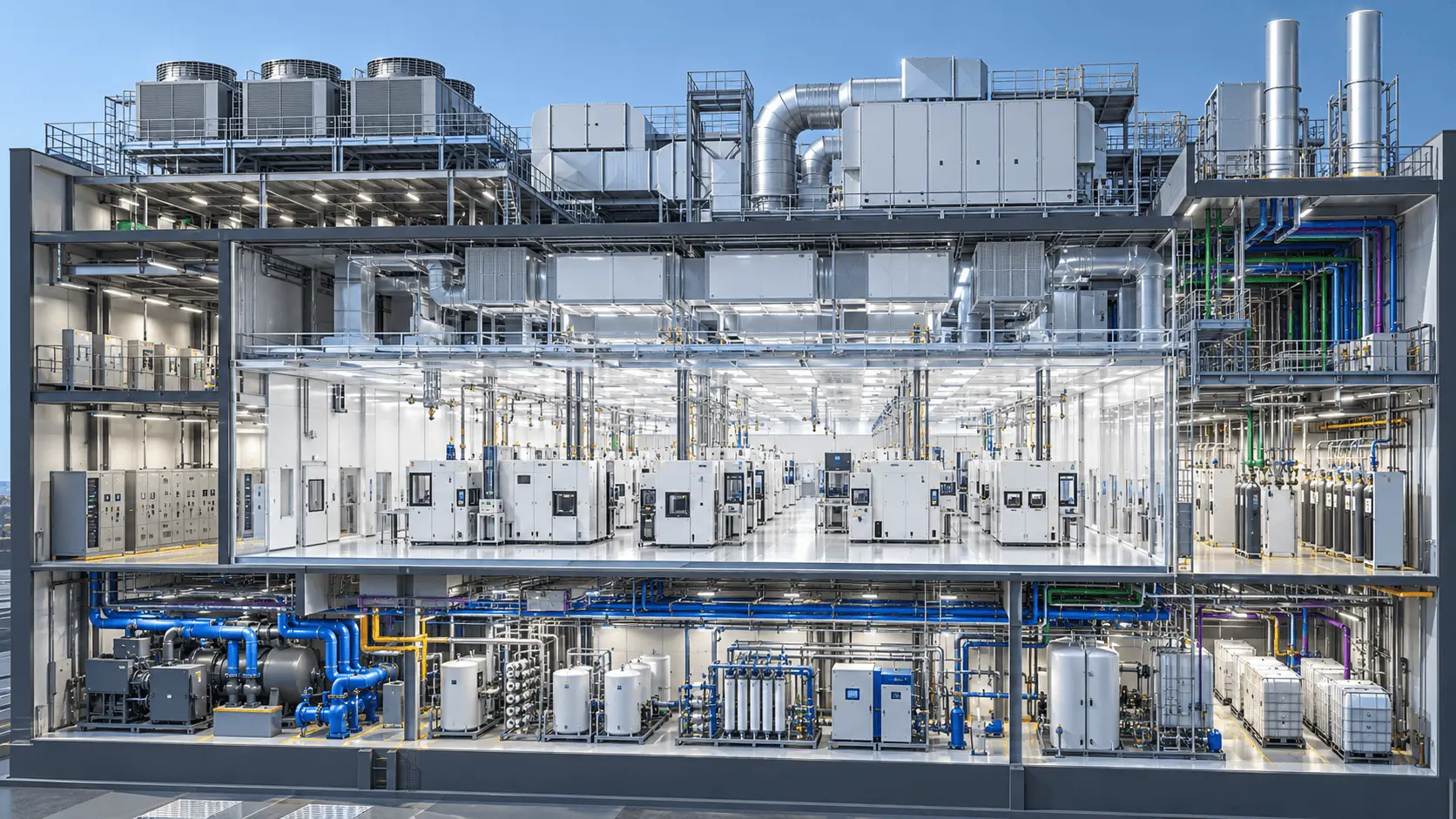
The manufacturing area depends on ventilation equipment, filtration, electrical systems, process piping, water treatment, gases, chemical distribution, exhaust, cooling, controls and many other supporting systems located around, above or below the production space.
A better way to think about a semiconductor cleanroom is therefore not as one room, but as part of a much larger engineered production environment.
What Does a Semiconductor Cleanroom Actually Control?
Particle control is usually the first thing people associate with cleanrooms, but contamination control is broader than simply removing visible dust.
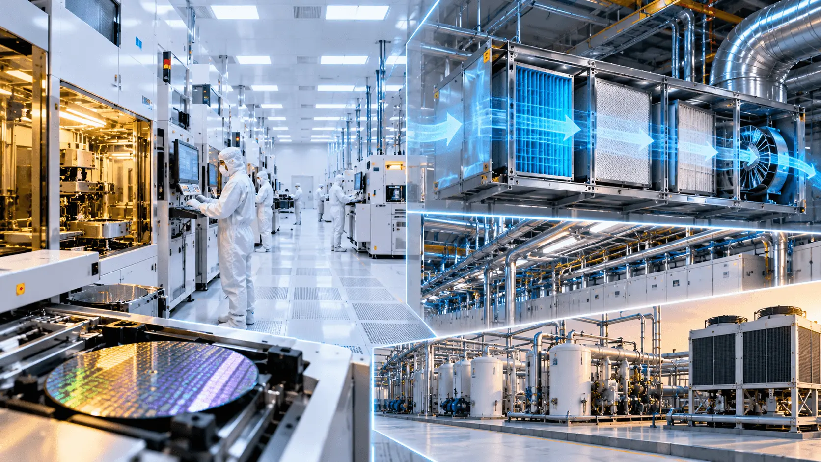
Air supplied to the production area must be filtered and continuously managed. Temperature and humidity may also need to remain within defined operating ranges because semiconductor processes and manufacturing tools are sensitive to environmental variation.
Air movement itself matters.
As an industry example,
Intel publicly explains that outside air entering one of its fabs is conditioned for temperature and humidity, filtered and then circulated through the cleanroom. Its published fab material describes air passing through the production area and being repeatedly filtered and recirculated.
Intel also explains that workers use specialised cleanroom clothing to reduce contamination from people, including hair, lint and skin particles.
That is useful for understanding the engineering principle, but Intel’s fab arrangement should not be treated as a published floor-by-floor design of Tata Electronics’ Dholera facility. Different fabs can have different layouts, equipment arrangements and process requirements.
The broader lesson is what matters: semiconductor contamination control involves the entire operating environment, not simply housekeeping.
People, materials, air movement, tool installation, piping cleanliness and maintenance activity can all become part of the contamination-control problem.
Cleanroom Air Has to Be Engineered Continuously
A semiconductor cleanroom cannot rely on cleaning the room once and then sealing the door.
The environment has to be maintained continuously.
Air-handling and filtration systems are designed to deliver clean conditioned air while controlling parameters required by the manufacturing environment. Depending on the design, large volumes of air may be recirculated through filtration systems while temperature and humidity are kept within the required range.
Pressure relationships between spaces may also be used to control how air moves between cleaner and less-controlled areas.
This creates an important construction distinction.
Installing walls, floors and ceilings does not prove that the cleanroom environment has been qualified.
The associated mechanical systems need to be installed, balanced, tested and demonstrated to perform as intended.
For readers following fab construction, a photograph of a finished ceiling or a clean-looking production area is therefore useful visual evidence of physical progress.
It is not, by itself, evidence that the complete environmental-control system has passed the required testing.
What Sits Behind the Semiconductor Manufacturing Area?
One of the easiest ways to understand fab infrastructure is to look beyond the manufacturing floor.
Intel’s public explanation of its own fabs provides a useful industry example.
Its layout describes a cleanroom supported by areas containing air-handling equipment, pumps, transformers, power systems, piping and utility infrastructure. Intel also describes large utility pipes carrying gases, liquids, exhaust and other services to and from manufacturing equipment.
Again, this should be read as an industry example, not as a drawing of the Dholera fab.
But it explains why so much semiconductor construction work can remain invisible in a normal exterior photograph.
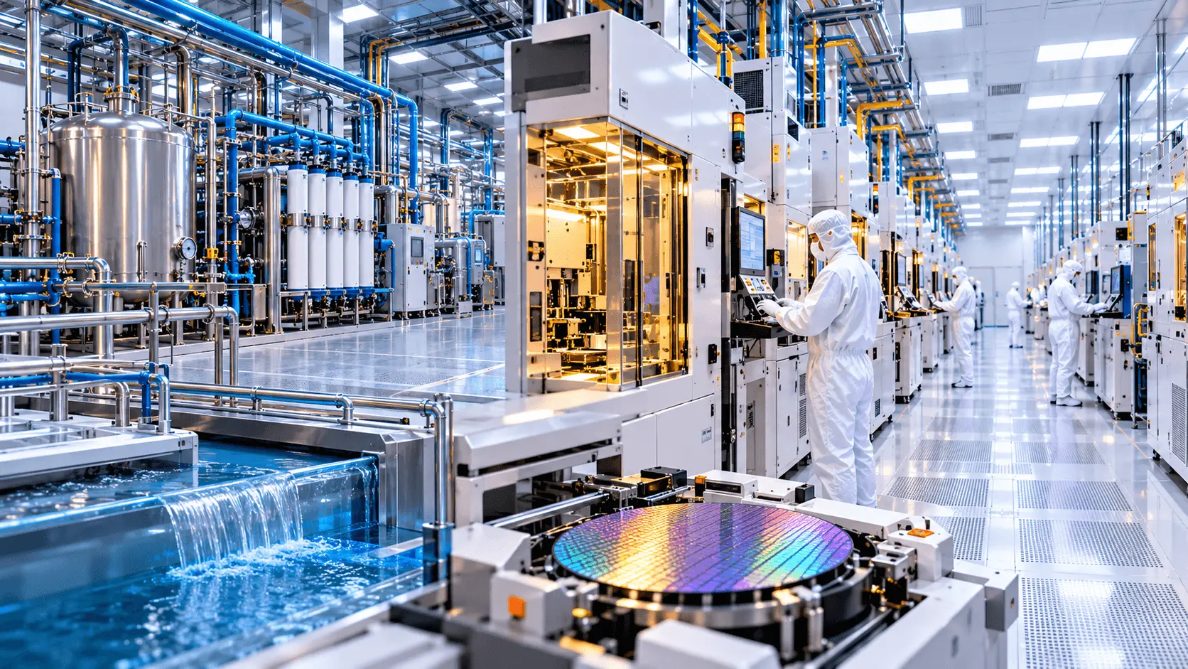
A process tool on the production floor may require connections to several services before it can operate.
Those connections can include electrical power, cooling, process water, compressed air, nitrogen, other gases, chemicals, vacuum or exhaust systems, depending on the specific equipment and manufacturing process.
Behind a clean manufacturing floor is therefore a dense engineering network.
That network is one reason semiconductor fabs are very different from conventional industrial sheds.
Why Ultra-Pure Water Matters
Ordinary municipal or industrial water is not suitable for many semiconductor process requirements.
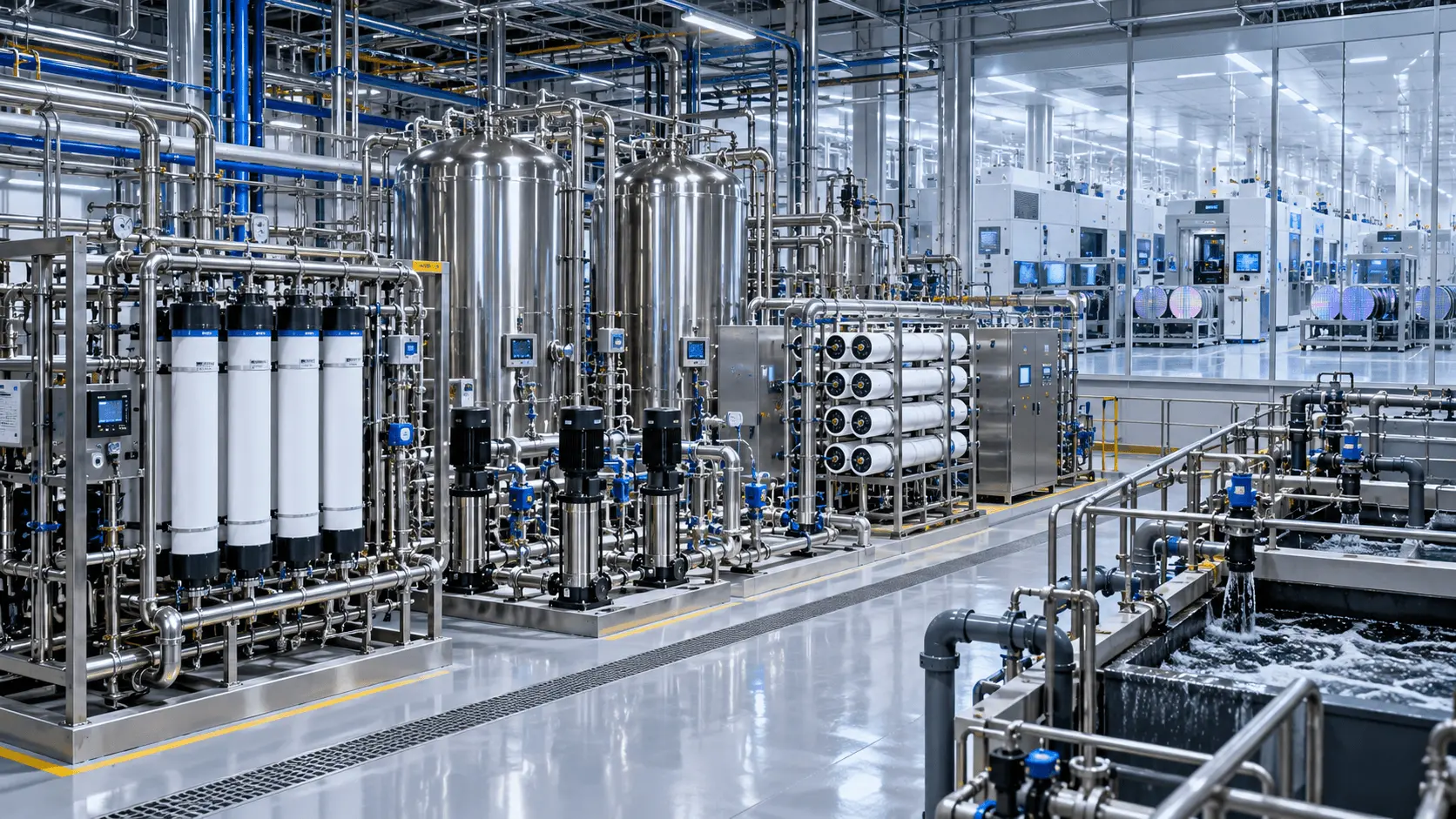
Semiconductor manufacturing uses highly treated water, commonly referred to as ultra-pure water or UPW, for process applications where dissolved minerals, particles, organic contamination and other impurities must be controlled to extremely low levels.
Creating that water requires considerably more than connecting the factory to a water pipeline.
A UPW system can involve several stages of treatment, storage, circulation and monitoring before water reaches manufacturing tools.
Waste streams also need their own treatment strategy because semiconductor manufacturing can generate different types of process wastewater.
This is directly relevant to Dholera.
A Tata Electronics project role advertised for Dholera in September 2026 specifically referred to the design, construction and operation of ultra-pure-water and wastewater-treatment systems for semiconductor production.
That is useful project-specific evidence that these systems form part of the engineering scope associated with the Dholera fab.
It should not be converted into a claim that the entire UPW system has been completed or commissioned unless Tata Electronics or another authorised project source separately confirms that milestone.
High-Purity Gases and Chemicals Are Another Hidden Layer
Semiconductor equipment can require a variety of gases and chemicals delivered under tightly controlled conditions.
This creates specialised requirements for piping, materials, joints, testing, leak integrity, cleanliness and distribution.
The role refers to high-purity and ultra-high-purity process systems and specifically mentions UPW, compressed dry air, nitrogen, specialty-gas distribution and chemical distribution.
It also refers to orbital welding, leak testing, particle-count testing, cleanroom construction protocols and material handling.
For someone trying to understand
Dholera semiconductor cleanroom infrastructure, this type of document is more informative than a distant photograph of the fab exterior.
It identifies the engineering disciplines being associated with the project.
But the distinction remains important: a job description tells us about project scope and responsibilities. It does not prove that every system described in that role has reached installation, commissioning or production readiness.
Tool Installation Is Different From Building Completion
A fab building ultimately exists to support semiconductor manufacturing equipment.
That equipment cannot simply be delivered, placed on the floor and switched on.
Production tools need to be positioned correctly and then connected, or “hooked up”, to the facility systems required for their operation.
Those connections can involve process piping, gases, chemicals, electrical services, cooling, exhaust and controls.
Tata Electronics’ September 2026 Dholera recruitment for a Tool Hook Up Program Manager refers directly to coordinating semiconductor equipment installation and utility integration. The role describes connections involving process piping, mechanical, electrical and chemical systems and also refers to cleanroom standards and equipment-readiness milestones.
That gives readers another useful way of judging semiconductor construction.
A building milestone and a manufacturing-equipment milestone are not the same milestone.
A fab may have substantial structural and cleanroom construction completed while still having major work ahead in equipment move-in, utility hookup, testing, qualification and production ramp-up.
Why a Completed Building Exterior Reveals So Little About Fab Readiness
This is probably the most important point for anyone following semiconductor construction through photographs or social-media updates.
The exterior tells you mainly about the exterior.
It can show that structural work has advanced. It may show roofing, cladding, utility buildings, roads, cooling structures or other visible construction.
Those are meaningful milestones.
But a photograph taken from outside normally cannot confirm whether a particular cleanroom has reached its required environmental conditions, whether high-purity piping has passed testing, whether UPW is available at the required quality, whether gas systems are commissioned, whether production equipment has been installed or whether process qualification has begun.
The closer a semiconductor facility gets to actual production, the more important the invisible engineering becomes.
This is why phrases such as “fab completed”, “cleanroom ready”, “equipment ready”, “production ready” and “commercial production started” should not be treated as interchangeable.
Each describes a different level of readiness.
What Current Dholera Evidence Can We Actually Point To?
There are several different levels of publicly available evidence around the Tata Electronics Dholera project.
At the project level, Tata Electronics has publicly stated that it is building a 300 mm semiconductor fab in Dholera in partnership with PSMC, with planned capacity of up to 50,000 wafers per month.
Tata has also announced partnerships relating to manufacturing equipment, process technology, factory automation and lithography for the Dholera facility.
More recently, September 2026 Tata Electronics recruitment material for Dholera has referred directly to cleanroom infrastructure, high-purity process piping, UPW, gases, chemicals, HVAC, tool hookup, testing, commissioning and semiconductor-project quality control.
Together, those sources help establish the type of engineering work associated with the project.
What they should not be used for is inventing an unsupported completion percentage.
Unless an authorised project source publishes a specific milestone, date or percentage with enough context to understand what has actually been completed, readers should resist filling that gap themselves.
That approach is less dramatic, but considerably more useful.
How Should Readers Judge a Claimed Cleanroom Milestone?
Construction updates become more credible when the claim and the evidence refer to the same thing.
If someone says structural work is progressing, an exterior site photograph may be perfectly reasonable evidence.
If the claim is that a cleanroom has achieved a defined readiness stage, the evidence should become more specific.
The same applies to utility commissioning, equipment move-in and production readiness.
A useful visual and documentary evidence guide is:
This approach is especially useful in semiconductor projects because so much important progress occurs inside controlled areas that the public may never see directly.
What Does “Ready for Equipment” Mean?
Readers may occasionally come across terms such as RFE, or Ready for Equipment, in semiconductor project material.
The basic idea is that the relevant facility area and supporting conditions have reached the point required for the next stage of equipment installation.
It should not automatically be translated as “the fab is ready for production.”
After equipment reaches its installation location, significant work can remain.
Tool hookup, utility connections, inspections, controls integration, testing, process qualification and manufacturing ramp can follow.
Tata Electronics’ Dholera tool-hookup recruitment material itself refers to Ready for Equipment dates as project milestones, which is a useful illustration of how equipment readiness sits within a broader project sequence.
What Is the Difference Between Cleanroom Readiness and Process Readiness?
Cleanroom readiness is primarily concerned with the controlled manufacturing environment and the facility systems supporting it.
Process readiness goes further.
The actual semiconductor process has to run reliably through its intended manufacturing steps. Production equipment, materials, recipes, controls, measurement systems and engineering teams all become part of that stage.
A cleanroom can therefore be an essential prerequisite without being the final proof of manufacturing readiness.
This distinction also explains why semiconductor-fab announcements should not be reduced to civil-construction photographs.
A fab is ultimately a combination of building infrastructure, precision utilities, advanced production tools and a qualified manufacturing process.
Frequently Asked Questions
Conclusion
Dholera semiconductor cleanroom infrastructure is best understood as an interconnected manufacturing system rather than a single clean room inside a factory.
The production environment depends on controlled air, contamination management and a large network of supporting infrastructure. Ultra-pure water, compressed dry air, nitrogen, specialty gases, chemicals, electrical systems, cooling, exhaust, wastewater treatment and equipment hookups can all sit behind the manufacturing floor.
Industry material from Intel helps explain how these systems support a semiconductor cleanroom in practice. It is useful as an industry example, not as a published design of the Dholera fab.
For Dholera itself, Tata Electronics’ public project information confirms the development of its 300 mm semiconductor fab, while its recent Dholera project roles provide useful evidence of the cleanroom, high-purity utility, water-treatment and tool-hookup engineering disciplines associated with the project.
Those sources still do not justify guessing a cleanroom-completion percentage or converting building progress into a production milestone.
For readers following future construction updates, the most useful habit is therefore simple: first identify exactly what is being claimed, and then ask whether the evidence actually proves that particular stage.
In semiconductor manufacturing, what happens behind the walls can matter more than what can be seen from the road.
Disclaimera
This article is for general educational and site-screening information. It is not legal, engineering, utility, tax, financial, investment or government-approval advice.
Descriptions of semiconductor cleanrooms, contamination control, utilities, tool hookup and manufacturing readiness are general engineering explanations. Actual specifications, cleanroom classifications, system designs, construction sequences and qualification requirements vary by facility, manufacturing process, equipment and project design.
References to Tata Electronics, PSMC, Intel or other semiconductor companies do not imply any partnership, endorsement or commercial association with Dholera City Buildconz.
Project details and engineering scope are based on company and government information publicly available at the time of writing. Recruitment notices describe roles, responsibilities and project work scopes; they should not be interpreted as proof that every referenced system has been completed, commissioned or placed into production.
No construction percentage, cleanroom-completion milestone, equipment-installation status or commercial-production date should be inferred unless supported by an authorised project or government source.
Dholera City Buildconz is an independent real estate consultancy/developer and is not affiliated with Tata Electronics, DICDL, DSIRDA or any Government authority.
Infrastructure development, industrial projects and semiconductor investment in Dholera should not be interpreted as a guarantee of property appreciation, rental income, investment returns or future demand. Property buyers should independently verify title, planning status, zoning, approvals and current government records before making any investment decision.